

The Olden Days
by Jon M Quigley
I recently had a phone call with a person I met on LinkedIn. Actually, I have been having calls with them over the weeks, to talk about product development, especially the way it was in the olden days. Over the course of few discussions we began chatting about work instructions, as that is what the company at which he works does. He demonstrated the tool, and I had flashbacks to the olden days. My first engineering job, was at a small custom industrial control company. We had to wear many hats. The company designed and manufactured products that were shipped around the world and in the states.
Rapid prototyping is not a new need nor is it a new idea. My first job after leaving university, was with a small control system company. This is where I met Tony Singleton. He worked as a part time consultant for the company at which I worked. I worked at the office during the day, and would drive to his house at night, where his wife would feed me (young and would often work through lunch and dinner) and we would go to his lab space and work. This is not memoriam of him, but he was the one who taught me (and many other younger engineers) and it is important to note this, especially from a principle perspective, that is the older folks sharing what they know.
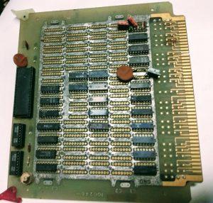
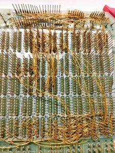
Figure 1 Wire wrapped board top and bottom (thank you Dusty Singleton for the photos).
Wire wrapping
Wire wrapping is an old-school method for building prototype products. Wire wrapping requires a perforated board. Either the bottom of the perforated board has extended legs, or each socket that contains long legs. These legs are lengthened that will allow wires to be wound around the leg. This wire is very thin, the tool below is used to strip the insulation from the wire, by pulling the wire through the notch. This stripped the insulation far enough back to ensure a good connection to the pin.
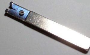
Figure 2 Wire stripping tool for wire wrapping.
A tool that looks like a screwdriver, but has a hole in the end that is used to wrap a small gauge wire around a post. To successfully build with this method, requires thinking upside-down and backwards. These very small gauge wires can also easily brake, which makes debugging a challenge when the underside of the boards resembles a rat or birds’ nest.
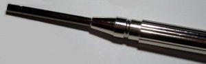
Figure 3 Wire wrapping tool.
With this technique, the board can be constantly developed, adding new portions to the design as we learn and add new features. In fact, that is what would happen. Developing a product in the olden day, in my experience, was never about building all of the product, then exercise the product and test. For example, we would prioritize adequate clocking of the microcontroller and set the inputs or outputs up to generically do something, press a button and the display engages. This tests the input, and the display software modules. We may find some prototype hardware errors, for example one of the circuits to the display may be wired in error, and the display presents not exactly what is being sent. These initial explorations of the product are as much about discovering prototype part anomalies as developing the software. I worked with 8051 microcontrollers, the windowed parts that allowed for erasing via ultraviolet light. This was before in circuit emulators (ICE), so to exercise the hardware required programming an actual chip. This means the debugging consisted of wire wrapped hardware, as well as software (assembly or C) that had successfully compiled. Trying to ascertain what is going wrong is difficult when you cannot see into the microcontroller or processor. It is demoralizing when you plug the programmed (software burned into the) microcontroller and nothing happens. Everything became significantly easier with the arrival of ICE.
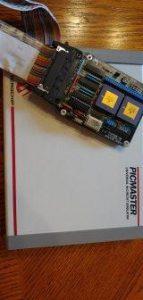
Figure 4 In Circuit Emulator (ICE)
In Circuit Emulators are substitutes for the microcontroller, and allows you to see what is going on inside the microcontroller. It became possible to set breakpoints, explore variables, and interact with the software as it is working in the product. Still requires prototype hardware, but rather than the programmed microcontroller, this device plugs into the prototype as if it were the micro into the chip carrier (socket), but you can readily explore the software and the hardware interactions, which makes debugging interrupts much easier and effective. The prototype was still built on perforated boards and wire wrapped, but that would change eventually.
Printed Circuit Boards
Eventually, we migrated from wire wrapping to creating our own prototype printed circuit boards (PCB), but it is not as easy as that sounds. This begins with creating a PCB from the schematic. A flat piece of copper clad fiberglass, no traces, one solid surface. The copper is covered with an exterior layer, that when exposed to ultraviolet light, will enable the etching or removal of the copper. A two-sided board then requires the top and bottom layers match in a way that completes the traces. This required a special eye to aligning the top and the bottom trace graphics (printed on vellum), then put into an ultraviolet chamber. Then the second layer print out would be put on the other side of the raw PCB. The entire board then went into a constantly agitated acid bath removing the copper that is not needed and leaving the traces on the top and the bottom. Rick Byrum was the only person that could align the top and bottom traces with the vellum to ensure the top trace, could connect to the bottom trace through a via (a plated hole on the printed circuit board into which no component is installed to transition a trace from one side of the board to the other). As there was no through-hole plating, we had to insert a small wire through any via, and solder to the top trace and to the bottom trace completing the connection. We got tired of agitating the acid bath manually, and Rick developed a way to keep the fluid constantly moving across the PCB by rocking the tray.
Work Instructions
This trip down memory lane comes with the manufacturing work instructions, for assembling the final resultant printed circuit board, that contained only through hole parts.. The manufacturing was largely manual labor, this includes stuffing the PCB. There was more to this assembly process than putting the PCB together, but that is where it started in this case.
There were multiple pages of 11×17 sized paper. The pages were bound on the left-hand short side, so they opened up from right to left, just like a book. Each page on the book had a graphic of the printed circuit board, along with installation instructions of which parts were installed where on the PCB. There would be a page for the integrated circuits, a page for all of the 4K resistors, 0.01μF capacitors and so on. Each page is used to install specific parts on the PCB, upon installing the parts on a specific sheet, that sheet is turned over, and the parts defined on the next sheet are installed. By the time the last sheet is turned, all of the parts are installed on the PCB. There would be another set of instructions integrating this subassembly into the other subassemblies such as the enclosure.
One of the recent discussions I had was with a company that creates modern work instructions systems where the presentment is via some display screen, no papers. The instructions are in the cloud and managed there and displayed out to the line workers, wherever they may be. In addition to controlling the introduction to the work instructions (change management), demonstration of the tools and equipment required is provided even before the work begins.
Things have Changed
So many of these things have changed, or at least there are many alternatives that do not seem to have been available in the olden days. One of the companies at which I have worked, Raptor Performance, is able to get prototype PCBs from China in a few days, no more etching, lining upper and bottom traces up and fabricating the vias, and no two-layer board limit. A finished production level looking board can be made and shipped in about 2 weeks. Perhaps we will never return to these earlier times, but this work presented younger engineers with great opportunities to learn.